Designing FPGAs Using the Vivado Design Suite 2
Course Description
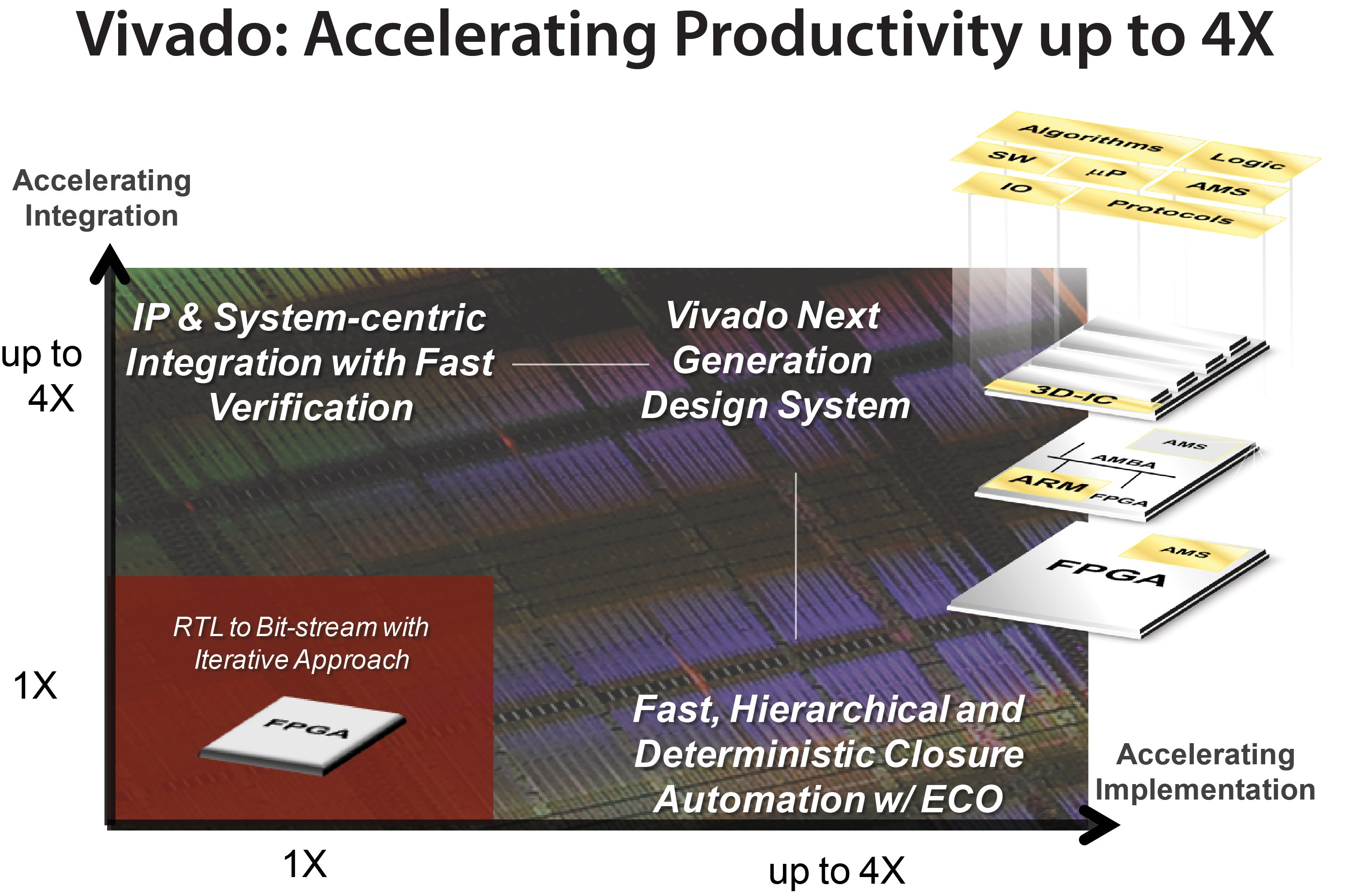
Learn how to build a more effective FPGA design:
The focus is on:
- Using synchronous design techniques
- Utilizing the Vivado® IP integrator to create a sub-system
- Employing proper HDL coding techniques to improve design performance
- Debugging a design with multiple clock domains
This course builds on the concepts from the Designing FPGAs Using the Vivado Design Suite 1 course.
 Level
Level
FPGA 2
Course Duration
2 days
Audience
Digital designers who have a working knowledge of HDL (VHDL or Verilog) and who are new to Xilinx FPGAs.
Prerequisites
- Basic knowledge of the VHDL or Verilog language
- Experience with the basics of the Tcl language
- Digital design knowledge
Optional Videos
Software Tools
- Vivado Design Suite 2022.1
Hardware
- Architecture: UltraScale™ and 7 series FPGAs*
- Demo board (optional): Zynq UltraScale+ ZCU104 board*
* This course focuses on the UltraScale and 7 series architectures. Check with your local Authorized Training Provider for the specifics of the in-class lab board or other customizations.
Skills Gained
After completing this comprehensive training, you will have the necessary skills to:
- Identify synchronous design techniques
- Build resets into your system for optimum reliability and design speed
- Create a Tcl script to create a project, add sources, and implement a design
- Describe and use the clock resources in a design
- Create and package your own IP and add to the Vivado IP catalog to reuse
- Use the Vivado IP integrator to create a block design
- Describe the Versal ACAP clocking architecture and hardware platform development using Vivado IP integrator
- Apply timing exception constraints in a design aspart of the Baselining procedure to fine tune the design
- Describe how power analysis and optimization is performed
- Describe the HDL instantiation flow of the Vivado logic analyzer
Course Outline
Day 1
- UltraFast Design Methodology: Design Creation –Overview of the methodology guidelines covered in this course. {Lecture}
- Synchronous Design Techniques –Introduces synchronous design techniques used in an FPGA design. {Lecture}
- Resets –Investigates the impact of using asynchronous resets in a design. {Lecture, Lab}
- Register Duplication –Use register duplication to reduce high fanout nets in a design. {Lecture}
- Clocking Resources –Describes various clock resources, clocking layout, and routing in a design. {Lecture, Lab}
- Versal ACAP: Clocking Architecture – Discusses the clocking architecture, clock buffers, clock routing, clock management functions, and clock de-skew. {Lecture}
- I/O Logic Resources –Overview of I/O resources and the IOB property for timing closure. {Lecture}
- Clocking and I/O Resources in the Versal ACAP – (Optional) Describes how to use the Clocking Wizard and Advanced IO Wizard to configure clocking subsystems and I/O subsystems, respectively, in the Versal ACAP. {Lab}
- Creating and Packaging Custom IP –Create your own IP and package and include it in the Vivado IP catalog. {Lecture, Lab}
- Using an IP Container –Use a core container file as a single file representation for an IP. {Lecture, Demo}
- Designing with the IP Integrator –Use the Vivado IP integrator to create the uart_led subsystem.
- Block Design Containers in the Vivado IP Integrator – Describes the block design container (BDC) feature and shows how to create a BDC in the IP integrator. {Lecture}
- Versal ACAP: Hardware Platform Development Using the Vivado IP Integrator – Describes the different Versal ACAP design flows and covers the platform creation process using the Vivado IP integrator. {Lecture, Lab}
Day 2
- Timing Constraints Editor –Introduces the timing constraints editor tool to create timing constraints. {Lecture}
- Report Clock Networks –Use report clock networksto view the primary and generated clocks in a design. {Lecture, Demo}
- Timing Summary Report –Use the post-implementation timing summary report to sign-off criteria for timing closure. {Lecture, Demo}
- Clock Group Constraints –Apply clock group constraints for asynchronous clock domains. {Lecture, Demo}
- Introduction to Timing Exceptions –Introduces timing exception constraints and applying them to fine tune design timing. {Lecture, Demo, Lab}
- Power Analysis and Optimization Using the Vivado Design Suite –Use report power commands to estimate power consumption. {Lecture, Lab}
- Configuration Process –Understand the FPGA configuration process, such as devicepower up, CRC check, etc. {Lecture}
- HDL Instantiation Debug Probing Flow –Covers the HDL instantiation flow to create and instantiate a VIO core and observe its behavior using the Vivado logic analyzer. {Lecture, Lab}
- Scripting in Vivado Design Suite Project Mode –Explains how to writeTcl commands in the project-based flow for a design. {Lecture, Lab}
- Design Analysis Using Tcl Commands –Analyze a design using Tcl commands. {Lecture, Demo, Lab}
![]()
Datum
09 november 2022 - 10 november 2022
Locatie
Core|Vision
Cereslaan 24
5384 VT
Heesch
Prijs
€ 0,00
of
20 Xilinx Training Credits
Informatie
Training brochure
Registratieformulier
Registratie op aanvraag, neem contact op met ons.