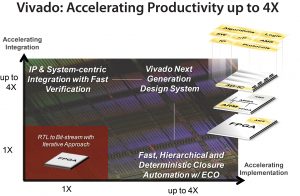
UltraFast Design Methodology
✅ indicates CONFIRMED TO RUN
Course Description
Learn how to improve design speed and reliability by using the UltraFast Design Methodology and the Vivado® Design Suite.
The focus is on:
- Optimizing system reset design and synchronization circuits
- Employing best practice HDL coding techniques
- Applying appropriate timing closure techniques
- Reviewing an UltraFast Design Methodology case study
 Level
Level
FPGA 3
Training Duration
2 days
Audience
Engineers who seek training for FPGA design best practices that increase design performance and increase development productivity.
Prerequisites
- Basic HDL knowledge (VHDL or Verilog)
- Digital design knowledge and experience
Software Tools
- Vivado Design Suite 2022.2
Hardware
- Architecture: UltraScale™ FPGAs*
- Demo board: None*
* This course focuses on the UltraScale and 7 series architectures. Check with your local Authorized Training Provider for specifics or other customizations.
Skills Gained
After completing this comprehensive training, you will have the necessary skills to:
- Describe the UltraFast™ design methodology checklist
- Identify key areas to optimize your design to meet your design goals and performance objectives
- Define a properly constrained design
- Optimize HDL code to maximize the FPGA resources that are inferred and meet your performance goals
- Build resets into your system for optimum reliability and design speed
- Build a more reliable design that is less vulnerable to metastability problems and requires less design debugging later in the development cycle
- Identify timing closure techniques using the Vivado Design Suite
- Describe how the UltraFast design methodology techniques work effectively through case studies and lab experience
Course Outline
Day 1
- UltraFast Design Methodology: Introduction – Introduces the UltraFast Design Methodology and the UltraFast Design Methodology checklist. {Lecture, Demo}
- UltraFast Design Methodology: Board and Device Planning – Introduces the methodology guidelines on board and device planning. {Lecture}
- Vivado Design Suite I/O Pin Planning – Describes the I/O Pin Planning layout for performing pin assignments in a design. {Lecture, Lab}
- Power Estimation Using XPE – Illustrates estimating the amount of resources and default activity rates for a design and evaluating the estimated power calculated
by XPE. {Lecture, Lab} - UltraFast Design Methodology: Design Creation – Introduces the UltraFast methodology guidelines on design creation. {Lecture}
- RTL Development – Covers RTL and the RTL design flow, recommended coding guidelines, using control signals, and recommendations on resets. {Lecture}
- Resets – Investigates the impact of using asynchronous resets in a design. {Lecture, Lab}
- Pipelining – Use pipelining to improve design performance. {Lecture, Lab}
- Synchronous Design Techniques – Introduces synchronous design techniques used in an FPGA design. {Lecture}
- Designing with the IP Integrator – Demonstrates how to use the Vivado IP integrator to create the uart_led subsystem. {Lecture, Lab}
- Creating and Packaging Custom IP – Covers creating your own IP and package and including it in the Vivado IP catalog. {Lecture}
- Revision Control Systems in the Vivado Design Suite – Use version control systems with Vivado design flows. {Lecture}}
Day 2
- UltraFast Design Methodology: Implementation – Introduces the methodology guidelines on implementation. {Lecture}
- Incremental Compile Flow – Utilize the incremental compile flow when making last-minute RTL changes. {Lecture}
- UltraFast Design Methodology Design Closure – Introduces the UltraFast methodology guidelines on design closure. {Lecture}
- Introduction to Vivado Reports Generate and use Vivado reports to analyze failed paths. {Lecture, Demo}
- Baselining – Use Xilinx-recommended baselining procedures to progressively meet timing closure. {Lecture, Lab}
- Clock Domain Crossing and Synchronization Circuits Use synchronization circuits for clock domain crossings. {Lecture}
- QoR Reports Overview Describes what quality of result (QoR) is and how to analyze the QoR reports generated by the Vivado IDE. {Lecture}
- Timing Closure Using Physical Optimization Techniques – Use physical optimization techniques for timing closure. {Lecture, Lab}
- Power Management Techniques Identify techniques used for low power design. {Lecture}
- Introduction to Floorplanning – Introduction to floorplanning and how to use Pblocks while floorplanning. {Lecture}
- Congestion – Identifies congestion and addresses congestion issues. {Lecture}
- Vivado Design Suite Debug Methodology – Understand and follow the debug core recommendations. Employ the debug methodology for debugging a design using the Vivado logic analyzer. {Lecture}
![]()
Datum
11 april 2023 - 12 april 2023
Locatie
Core|Vision
Cereslaan 24
5384 VT
Heesch
Prijs
€ 0,00
of
20 Xilinx Training Credits
Informatie
Training brochure
Registratieformulier
Registratie op aanvraag, neem contact op met ons.