Designing FPGAs Using the Vivado Design Suite 4
Course Description
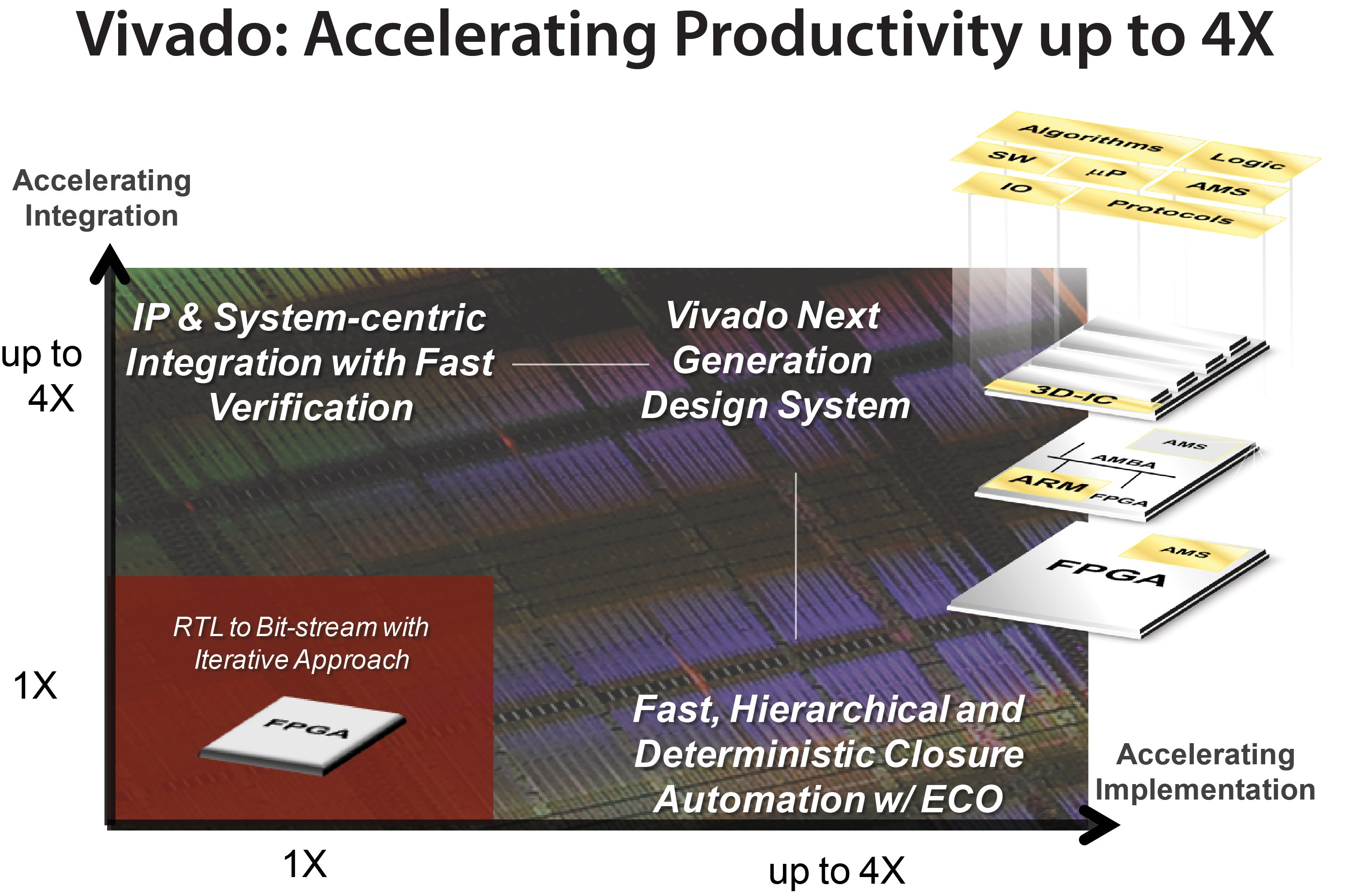
This course tackles the most sophisticated aspects of the Vivado® Design Suite and Xilinx hardware. This course enables you to use the advanced capabilities of the Vivado Design Suite to achieve design closure.
 Level
Level
FPGA 4
Course Duration
2 days
Audience
Prerequisites
- Designing FPGAs Using the Vivado Design Suite 2 course
- Designing FPGAs Using the Vivado Design Suite 3 course
- At least six months of design experience with Xilinx tools and FPGA
Software Tools
- Vivado System Edition 2018.3
Hardware
- Architecture: UltraScale™ and 7 series FPGAs*
- Demo board (optional): Kintex® UltraScale FPGA KCU105 board or Kintex-7 FPGA KC705 board*
* This course focuses on the UltraScale and 7 series architectures. Check with your local Authorized Training Provider for the specifics of the in-class lab board or other customizations.
Skills Gained
After completing this comprehensive training, you will have the necessary skills to:
- Apply appropriate I/O timing constraints and design modifications for source-synchronous and system-synchronous interfaces
- Analyze a timing report to identify how to center the clock in the data eye
- Use Tcl scripting in non-project batch flows to synthesize, implement, and generate custom timing reports
- Utilize floorplanning techniques to improve design performance
- Employ advanced implementation options, such as incremental compile flow, physical optimization techniques, and re-entrant mode as last mile strategies
- Utilize Xilinx security features, bitstream encryption, and authentication using AES for design and IP security
- Identify advanced FPGA configurations, such as daisy chain and gangs, for configuring multiple FPGAs in a design
- Debug a design at the device startup phase to debug issues related to startup events, .such as MMCM lock and design coming out of reset
Course Outline
Day 1
- UltraFast Design Methodology: Advance Techniques {Lecture}
- Scripting in Vivado Design Suite Non-Project Mode {Lecture, Lab}
- Hierarchical Design {Lecture}
- Managing Remote IP {Lecture, Lab}
- I/O Timing Scenarios {Lecture}
- Source-Synchronous I/O Timing {Lecture, Lab}
- System-Synchronous I/O Timing {Lecture, Demo}
- Timing Constraints Priority {Lecture}
- Case Analysis {Lecture}
- Introduction to Floorplanning {Lecture}
- Design Analysis and Floorplanning {Lecture, Lab}
- Incremental Compile Flow {Lecture, Lab}
Day 2
- Physical Optimization {Lecture, Lab}
- Vivado Design Suite ECO Flow {Lecture, Lab}
- Power Management Techniques {Lecture}
- Daisy Chains and Gangs in Configuration {Lecture}
- Bitstream Security {Lecture, Lab}
- Vivado Design Suite Debug Methodology {Lecture}
- Trigger and Debug at Device Startup {Lecture, Demo}
- Debugging the Design Using Tcl Commands {Lecture, Lab}
- Using Procedures in Tcl Scripting {Lecture}
- Using Lists in Tcl Scripting {Lecture}
- Using regexp in Tcl Scripting {Lecture, Lab}
- Debugging and Error Management in Tcl Scripting {Lecture}
Topic Descriptions
Day 1
- UltraFast Design Methodology: Advance Techniques –Introduces the UltraFast™ design methodology guidelines covered in this course.
- Scripting in Vivado Design Suite Non-Project Mode – Write Tcl commands in the non-project batch flow for a design.
- Hierarchical Design – Overview of the hierarchical design flows in the Vivado Design Suite.
- Managing Remote IP – Store IP and related files remote to the current working project directory.
- I/O Timing Scenarios –Overview of various I/O timing scenarios, such as source- and system-synchronous, direct/MMCM capture, and edge/center aligned data.
- Source-Synchronous I/O Timing – Apply I/O delay constraints and perform static timing analysis for a source- synchronous, double data rate (DDR) interface.
- System-Synchronous I/O Timing – Apply I/O delay constraints andperform static timing analysis for a system -synchronous inputinterface.
- Timing Constraints Priority – Identify the priority of timing constraints.
- Case Analysis – Understand how to analyze timing when usingmultiplexed clocks in a design.
- Introduction to Floorplanning – Introduction to floorplanning and how to use Pblocks while floorplanning.
- Design Analysis and Floorplanning–Explore the pre- and post- implementation design analysis features of the Vivado IDE.
- Incremental Compile Flow – Utilize the incremental compile flow whenmaking last – minute RTL changes.
Day 2
- Physical Optimization – Use physical optimization techniques for timing closure.
- Vivado Design Suite ECO Flow – Use ECO flow to make changes to a previously implemented design and apply changes to the original design.
- Power Management Techniques – Identify techniques used for low power design.
- Daisy Chains and Gangs in Configuration –Introduces advanced configuration schemes for multiple FPGAs.
- Bitstream Security – Understand the Xilinx bitstream security features such as readback disable, bitstream encryption, and authentication.
- Vivado Design Suite Debug Methodology – Understand and follow the debug core recommendations. Employ the debug methodology for debugging a design using the Vivado logic analyzer.
- Trigger and Debug at Device Startup – Debug the events around the device startup.
![]()
Datum
21 november 2019 - 22 november 2019
Locatie
Core|Vision
Cereslaan 24
5384 VT
Heesch
Prijs
€ 0,00
of
18 Xilinx Training Credits
Informatie
Training brochure
Registratieformulier
Registratie op aanvraag, neem contact op met ons.